This article reflects the opinion and analysis as well as information collated by AE Research Management Sdn Bhd, and does not constitute an investment advice or recommendation
From the exponential rise in stock prices of EUV (extreme ultra-violet) semiconductor equipment makers since 2018, one would surmise that EUV lithography is the long-awaited quantum leap in front-end process that will enable the continuation of Moore’s law (node shrinkage).
However, EUV will not be the sole dynamics that dictate semiconductor advancements through the 2020s. Much depends also on ‘mundane’ but mission-critical processes such as wafer testing, grinding and dicing (cutting). As precision specifications reach the micron (one-millionth of a meter) level, core technological capabilities lie with only a very small number of firms.
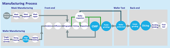
Wafer Electrical Testing
Prior to EUV in 2019/2020, the most advanced lithography process was ArF immersion introduced circa 2005. As the ArF process became matured through the 2010s, semiconductor makers were able to continually improve on their front-end yield, thus require lesser wafer testing.
EUV represents a transformational process that will become even more challenging when logic nodes shrink to 2-4 nm (from current 7-10nm), necessitating high NA (numerical aperture) configurations. With newer front-end processes, demand for wafer electrical test should expand.
Another driver for longer duration and more extensive testing, is the growth of automotive and industrial-use ICs, where ultra-reliability takes on a different order of importance compared to consumer ICs (those used in smartphones).
In addition, the industry is adopting newer architectures such as SiP (system-in-package) and chiplets (details below) which will result in substantial increase in the number of raw dies, and hence electrical testing requirements for the dies.
Like many areas of deep science & engineering, the supplier base has become oligopolistic. For semiconductor wafer electrical testing, the probe machines are dominated by Tokyo Seimitsu and Tokyo Electron, controlling over 95% market share. Barriers to entry emanate from precision positioning and rigidity required of these machines, which necessitate proprietary system design, in-house machine tools and excellent craftmanship.
Grinding and Dicing
Equally crucial to further the semiconductor roadmap are grinding and dicing (cutting) technologies. Like wafer testing, grinding and dicing systems are dominated by only 2 players – DISCO Corporation and Tokyo Seimitsu.
In the 1960s, semiconductor silicon wafer was only 23mm in diameter, and 275 microns in thickness. Following the development of larger silicon ingots to match the increase demand of chips and cost reduction, wafer diameter was shifted to 125mm in 1981, then a transition to 200mm in 1992, followed by 300mm since the 2000s. Although bigger wafer can fit in more chips per wafer, this comes at a cost. The wafer has to get thicker due to the difficulty of cutting a large-area wafer from an ingot – wafer thickness now ranges from 725 – 775 microns, almost triple the original thickness. For the next generation 450mm diameter wafer, thickness will reach 925 microns.
The thicker wafers get, the more frontside/backside grinding they need. Chips thickness varies by applications – logic wafers are grinded down to 100 microns, while DRAM and NAND can be as thin as 30-50 microns. This means about 650-700 microns of grinding from the current thickness!
Grinding is necessary for numerous reasons. A thinner chip has the advantage of limiting the movement of electrons, resulting in lesser resistance and power consumption.
It also provides more space for other components to fit into a compact device. For example, memory company wants to get their chip as thin as possible (stretching to 20-30 microns thickness per chip), in order to stack more chips to form a 3D/multi-chip package (see graphic below).
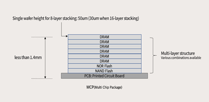
In such a case, uniformity requirement is extreme with tolerance of less than 1 micron. An uneven thickness of grinded chips cannot be stacked and might malfunction during use.
For ease of handling, wafer edge is grinded for smoothness. Silicon in crystalline state is very brittle and breaks off easily when grip forces are applied to a rough edge during fabrication steps. A breakoff wafer can contaminate other chips or damage expensive manufacturing system.
Semiconductor dies are cut out from the thinned wafers in a process called dicing, either via a mechanical or optical process. In mechanical method, diamond-binded blades are used to saw through the wafer on scribe line (space between die) of less than 100 micron. Precision has evolved to the equivalent of grooving a human hair crosswise some 30 times!
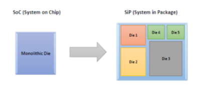
Demand for dicing equipment will be boosted by preference towards multi-die architectures (such as SiP, 3D stacking and chiplets) instead of ever larger monolithic SoC (system-on-chip). Since SoC has to be fabricated on the same single die, expensive node technology is applied to every functions on the chip, which may not be optimal in terms of cost and complexity. Instead, by applying the right node technology to each specific functions and combining them into a single SiP for example, manufacturing cost can be reduced without sacrificing overall performance. With greater number of dies than otherwise (see below), the volume of wafer dicing will inevitably increase.
With the electricfication of automobiles and introduction of 5G communication network, semiconductors are increasingly used in high voltage and ultra-high frequency applications. This will necessitate semiconductors to be fabricated on SiC (silicon carbide) or GaN (gallium nitride) wafers, which are harder substance to cut (and grind) than silicon.
Continual node shrink has meant chips become denser over time. Such packed wiring in transistor-dense chip requires good insulating materials, in order to maintain low crosstalk and signal performance. The industry has adopted low-k (dielectric) materials to solve the interconnect issues. However, these are fragile ceramics or porous materials inside the chip structure, thus prone to crack during blade dicing – a small stress from the sawing process will cause damage to a functional chip. Alternatively, laser and plasma dicing techniques can be adopted to reduce the stress and enhance dicing yield, albeit at higher costs.